U.S. CHIPS and Science Act
The act provides new funding to boost domestic research and manufacturing of semiconductors in the United States.


What Is the CHIPS and Science Act of 2022?
The U.S. CHIPS (Creating Helpful Incentives to Produce Semiconductors) and Science Act is a $52.7 billion plan signed by United States President Joseph (Joe) Robinette Biden Jr.
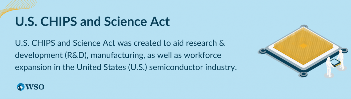
The U.S. CHIPS and Science Act was created to aid research & development (R&D), manufacturing, as well as workforce expansion in the United States (U.S.) semiconductor industry.
The CHIPS Act was passed in an effort to make the United States more competitive in the global semiconductor space with Asian powerhouses such as China, South Korea, Japan, and Taiwan.
Additionally, PwC states that U.S. semiconductor manufacturing capacity has dropped from nearly 40% of global supply in 1990 to 12% today). While the United States used to be one of the world’s leaders in semiconductor manufacturing, most production has been outsourced to companies like TSMC overseas in recent years.
For this reason, any country deemed a national security threat to the U.S. is deemed a restriction for a place of expansion for those receiving funding from the CHIPS Act.
Additionally, as we dream about the future – whether it is new innovations such as AI or quantum computing or enhanced items we use every day, such as computers, medical devices (MedTech), or planes – all eyes point to semiconductors as the backbone of our dreams.
- The U.S. CHIPS Act is a $52.7 billion plan signed by President Joe Biden.
- It aims to boost the U.S. semiconductor industry through R&D, manufacturing, and workforce expansion.
- The act addresses national security and supply chain concerns.
- Semiconductors are crucial for modern technology, including AI, cars, and everyday devices.
- Understanding semiconductor subsectors is valuable in technology investment banking.
- Moore's Law drives semiconductor advancements.
- Smaller semiconductor companies can benefit from the CHIPS Act's support.
Semiconductors
In the U.S., much of the design work happens here for semi-production. Japan and China typically create the raw products and elements for the semis.

Finally, the assembly, testing, and packaging usually happen at a place outside the U.S., like Taiwan (TSMC – for the world’s main foundry, see the chart below) or South Korea.
As you can likely see from the above descriptions, we need the CHIPS Act because we aren’t so dependent on other countries if there is a global crisis.
What exactly is a Semiconductor? A Core Subsector of TMT Investment Banking? Before we tackle the details of the CHIPS ACT, we should first answer your likely question: “what even is a semiconductor?”
You’ve likely heard that semiconductors are “what powers your iPhone,”; but what exactly does that even mean and what even is a semiconductor?
A semiconductor (or “semi” for short) is a small electronic device that is made up of billions of individual components that enable the storage, processing, as well as movement of data.
Note
It is also worth noting that semiconductors are typically smaller than a stamp that you would use for mailing letters and packages.
The invention of the transistor in the early 1950s allowed for the consistent flow of electricity for the first time.
From there, mankind developed the integrated circuit in 1958, which allowed hundreds of thousands of resistors, inductors, and transistors to be “printed” onto the silicon material, which is the modern semi we know and love today.
Most recently, the trend over the years points to semis becoming more and more compact, allowing for an increase in complex integrations of semi-products.
So, we hope you better understand how powerful semiconductors are and why the U.S. CHIPS and Science Act can be of such use.
Note
Semiconductors are typically made up of either silicon or germanium, the preferred material is silicon (hence the “Silicon” in Silicon Valley, California, USA).
This is because of silicon’s ability to withstand higher temperatures, its abundance in nature, and its inexpensive nature.
As an investment banker in the TMT or global technology space, you are likely to encounter at least one deal that has to deal with semis, such as Broadcom’s acquisition of VMware for $61 billion.
While semis might not be the first sub-sector that comes to mind when talking about tech banking, it sure may help you better appreciate how diverse the entire TMT space truly is. Subsectors of the Semiconductor Industry that the U.S. CHIPS Act Will Positively Impact.
Categories of a Semiconductor
In today’s world, there are primarily 4 categories that a semiconductor can fall into. The U.S. CHIPS is used to fund all 4 categories as listed below.
It’s important to understand all categories as you get a better understanding of truly how involved semis are in our everyday lives
While we won’t get into the granular “science” behind these tiny yet powerful devices, it’s in your best interest that you have a solid foundation on the various types of semiconductors out there that you may come across without even realizing in your daily lives.
Ordered by their contribution to total semiconductor sales (measured in $USD), the subsectors are as follows:
1. Microprocessors and Logic Devices [~40% of sales]:
These kinds of semis are primarily used for the most common in consumer electronics such as computers and smartphones (think iPhones).
This subcategory deals with the most complex forms of data manipulation whose concepts would go over both of our heads!
2. Memory Devices [~25% of sales]:
These kinds of semis are primarily used to store data instead of manipulation from microprocessors and logic devices.
3. Optoelectronics, Sensors, and Discretes (O-S-D) [~22% of sales]:
"O” in optoelectronics and “S” in sensors are used for sensing and generating (the prefix “opto-” often refers to vision – so, think cameras!).
The “D” in the “O-S-D” acronym stands for discrete (e.g., transistors, diodes, and resistors), which essentially means “separate”.
So, it’s best for these kinds of semis as those that can only perform a singular, unique electrical function.
4. Analog Devices [~13% of sales]:
These kinds of semis are primarily used to translate analog signals (i.e., light, voice command, touch, etc.). It’s best to think of these kinds of devices as those which would enable you to record yourself speaking
Fabless vs. Foundry & IDMs - Why they matter
We understand that you may have further questions on the different types of semis that are in the industry, so we included a table below that shares
| Fabless | Foundry (a.k.a. “Fab” for short) | Integrated Device Manufacturer (IDM) | |
|---|---|---|---|
| Common question that is asked for each category of semis | “I’ve heard the term ‘fabless’ before; what exactly does that mean?” | “I’ve heard the term ‘foundry’ before; what exactly does that mean?” | “So, are there any companies out there that may do both?” |
| Simple Definition (in Plain English) | Fabless refers to the designing/creation of semis (will outsource production to 3rd party like TSMC) | Foundry refers to the actual production/manufacturing process of semis | IDM refers to companies that BOTH design as well as manufacture semis |
| Key Players | Think NVIDIA (USA), AMD (USA), Broadcom (USA), or Qualcomm (USA) | Think GlobalFoundries (USA) or TSMC (Taiwan) | Think Intel (USA) or Samsung (South Korea) |
While a majority of the companies mentioned above are in fact from the United States, it’s clear that a generous package like the U.S. CHIPS and Science Act was needed.
Furthermore, the semiconductor industry is such an R&D (research & development) and CapEx -intensive (capital expenditures refers to the spending on long-term fixed assets like equipment or machinery).
When we implement something like the CHIPS Act, we truly address the main issue of the semi-industry, the supply chain problem…
Throughout the 21st century and specifically during 2022, the tension (economic and political) between China and the U.S. caused the U.S. to address national security concerns and supply chain issues if something were to happen overseas with Taiwan or China.
To address your concern up front, we chose to cover such a historic event in American history because the most popular industry coverage group in investment banking is far and away from the TMT group.
Note
The acronym TMT stands for technology (“tech”), media, & telecommunications (“telecom”).
Now, within the technology sector, we have the following 5 subsectors:
- Internet
- Software
- Hardware/ equipment
- IT services
- Semiconductors.
The U.S. CHIPS and Science Act is a major technology trend found in the semiconductor industry.
Purpose of U.S. CHIPS and Science Act
If you’re not already familiar with Moore’s Law, then now is probably the best time to get you up to speed so that you can better understand how the modern technology landscape came to be in today’s society.
Undoubtedly, you and I value semis so much – hence the medium likely chosen to read this content is via a technological advancement computer or smartphone).
Not only have we seen semis enter futuristic ideas and industries like artificial intelligence (AI) and high-tech militaristic devices, but we are also beginning to see them enter the everyday products we use, such as our cars.
For instance, 30 to 40% of the production cost of the newest cars comprises electronic systems containing semis. When we compare this range to 4 to 5 years ago, we see that these electronic systems merely only made up about 10 to 20% of the total cost of these systems.

Moore’s Law is a general rule of thumb that states computational power will become faster, more compact, and, as you likely already guessed, much much more cost-effective, approximately every 18 months – and yes, that means cheaper price tags for me and you!
A big question many students tend to have with the semi-industry is if there are any instances of smaller, lesser-known companies out there that can thrive.
In short, yes, as chips become ever more relevant in older mechanical industries, there is a growing need for more foundries in the U.S.
A specific example that we can point to is SkyWater Technology, the only truly pure-play U.S. fab that is also entirely U.S. owned.
SkyWater is based in the U.S., and they have special military contracts for unique militaristic needs. As you can see, the CHIPS Act only amplifies these smaller, “non-household” semi-companies based in the U.S.
U.S. CHIPS and Science Act Vs. Finance
The U.S. CHIPS and Science Act is a technology trend at the end of the day, but that’s what makes it so unique. The CHIPS and Science Act directly helps fund these facilities to create semis (fabless or foundry).
The entire semi-production industry is heavily CapEx-intensive (high capital expenditures on PP&E). Typically at these factories, advanced robots are the only ones that will be creating/assembling the semis.
As you likely already know, the semiconductor industry is just 1 of the 5 sub-sectors in the technology sector – the other 4 being
- the internet,
- software,
- hardware/equipment, and
- IT services.
Being knowledgeable in various technology trends (such as the U.S. CHIPS Act) is bound to give you a leg up in technology, media, & telecommunications (TMT) investment banking interviews.
Common global technology / TMT investment banking interview questions may include:
- “Tell me about a tech trend that you’ve been following.”
- “Can you describe the outlook on the semiconductor industry?”
As a response, you can most definitely talk about semis and the CHIPS Act now that you have a better appreciation of how diverse the technology sector truly is than when you first clicked on this article. You still believed that TMT merely FAANG companies.
The key message we want you to grasp is that semiconductors are at the heart of today's and future innovation. The CHIPS Act significantly enhances all potential aspects of design and innovation.
U.S. CHIPS and Science Act FAQ

The U.S. CHIPS Act is designed to promote the development and growth of the computer hardware, information technology, and consumer electronics industries in the United States.
It provides funding for research and development, grants and loans for small businesses, tax incentives, and export promotion activities to help these industries succeed.
The Office of Technology Policy (OTP) within the Department of Commerce is responsible for coordinating the implementation of the U.S. CHIPS Act and providing guidance to businesses in the computer hardware, information technology, and consumer electronics industries.
Yes, there are many other science-related acts in the United States. Some examples include
- The National Science Foundation Act, which establishes the National Science Foundation and provides funding for scientific research;
- The National Institutes of Health Act, which establishes the National Institutes of Health and provides funding for biomedical research; and
- The National Aeronautics and Space Act, which establishes the National Aeronautics and Space Administration (NASA) and provides funding for space exploration.
These science-related acts provide funding for scientific research and establish agencies to support and promote the advancement of science in the United States.
They also establish policies and goals for scientific research and provide resources and support to researchers and institutions conducting scientific research.


or Want to Sign up with your social account?